This is the PCF8591 a single chip single supply, low power 8bit CMOS data acquisition device with four analog inputs. 1 analog output and i2c Serial communication bus interface that allows the connection to be connected in series integrated bus for a maximum of 127 units. The PCF8591 has three addresses the pin A0, A1, A2 are used for programming the hardware address allows you to hookup up to 8 device connected to the i2C but without additional hardware. Address control and data to and from the device are transferred serially via the two-line bidirectional i2C bus.
The functions of the device has an analog input multiplexing on-chip track and hold function 8bit analog-to-digital conversion and an 8bit digital to analog conversion. The maximum conversion rate is given by the maximum speed of the i2c Bus. The PCF8591 can be used in closed loop control system, low power converter for remote data acquisition, battery operated equipment, and Acquisition of analog values in automotive, audio and TV applications.
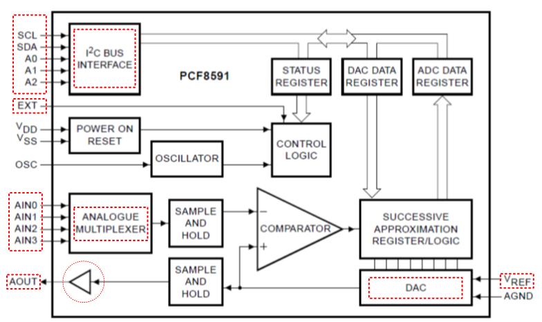
PCF8591 Block Diagram
To identify the i2C address of the device used the pin A0, A1, or A2. The selection of the ADC channel that you want to use is selectable via the control byte register and configurable via software as well as the Analog Output Management. refer to PHILIPS PCF8591 DAC Datasheet

Required Component
- Arduino Micro-controller, ATTINY, TEENSY, ESP8266,
- PCF8591 DAC / PCF8591 Break Out Board
- Solderless Bread
- Jumper Wire / DuPont Wire
- 10k Potentiometer
- DS18B20 (To test the Digital to Analog Conversion)
Tested on
- ATMEGA328 16/12
- ATMEGA32u4 16/8/ MHz
- ESP8266
- ATMEGA250 16 MHz
- ATSAM3x8E
- ATSAM21D
- ATTINY85 16/8 MHz
Wiring Guide (See the circuit diagram below that uses an integrated PCF8591 and the Arduino NANO Microcontroller Board)

The 4 significant BITS are fixed and cannot be changed while the 3 significant fits are precisely connected to pin A0, A1, and A2. We can get the device address to the following binary value.
0b1001000 which is converted in HEX value 0x48
Once the address is set, you need to configure the device via CONTROL BYTE register. The values to be assigned to the control byte to select various analog input configuration in 4 single-ended inputs (Bit4 and Bit5 to Zero) will be:
- 0b00000000 > 0x00 > Active Analog Fattening AINO
- 0b00000001 > 0x01 > Active Analog Fattening AIN1
- 0b00000010 > 0x02 > Active Analog Fattening AIN2
- 0b00000011 > 0x03 > Active Analog Fattening AIN3
See below the sequence of byte to be sent.

The necessary instructions you can send the i2C bus a 1st byte containing the address of the device and a second byte in the internal configuration of the device. The PCF8591 is ready to scan and send the data to the i2C channel. The following code below allows you to capture a given analog AIN0 and AIN1 sending back to serial monitor.
For more details please refer to the Datasheet
Source Code
|
1 2 3 4 5 6 7 8 9 10 11 12 13 14 15 16 17 18 19 20 21 22 23 24 25 26 27 28 29 30 31 32 33 34 35 36 37 38 39 |
#include <Wire.h> void setup () { Wire.begin (); Serial.begin (9600); Serial.begin(9600); Serial.println("14CORE | Start DAC(Digital to Analog Convertion Test Code"); Serial.println("=========================================================="); Serial.println("Starting ....") Serial.println("") } void loop () { Wire.beginTransmission (0x48); //Start write request address 0x48 Wire.write (byte (0x00)); //Send config bytes set anable AIN0 Wire.endTransmission (); //Set end transmit Wire.requestFrom (0x48, 1); //Request byte slave address 0x48 while (Wire.available ()) //Set availability data bus { bytes Wire.read c = (); //Read byte from PCD8591 Serial.println (c); //Send data to serial monitor } delay (10); //Break delay 10 miliseconds Wire.beginTransmission (0x48); //start write request address 0x48 Wire.write (byte (0x01)); //Send the configuration bytes enable AIN01 Wire.endTransmission (); Wire.requestFrom (0x48, 1); while (Wire.available ()) { bytes Wire.read c = (); //Read data a / d conbertion pin AIN01 Serial.println (c); } delay (1000); } |
Downloads